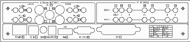
Connectors and controls on the rear panel are:
| Pos: | Symbol | Description: | |||||||||||||||||||||||||||||||||||||
|---|---|---|---|---|---|---|---|---|---|---|---|---|---|---|---|---|---|---|---|---|---|---|---|---|---|---|---|---|---|---|---|---|---|---|---|---|---|---|---|
| on the rear panel | in the Manual | ||||||||||||||||||||||||||||||||||||||
| 1 | POWER | Power switch | |||||||||||||||||||||||||||||||||||||
| 2 | DC IN | Power supply connector | |||||||||||||||||||||||||||||||||||||
| 3 | AGND | Ground connector | |||||||||||||||||||||||||||||||||||||
| 2048 kbit/s PCM_INTERFACE: | |||||||||||||||||||||||||||||||||||||||
| 8 | Tx | PCMTA | PCM_INTERFACE port 'A' output (balanced 120 Ohm) | ||||||||||||||||||||||||||||||||||||
| 9 | Rx | PCMRA | PCM_INTERFACE port 'A' input (balanced 120 Ohm) | ||||||||||||||||||||||||||||||||||||
| 10 | Tx | PCMTA | PCM_INTERFACE port 'A' output (unbalanced 75 Ohm) | ||||||||||||||||||||||||||||||||||||
| 11 | Rx | PCMRA | PCM_INTERFACE port 'A' input (unbalanced 75 Ohm) | ||||||||||||||||||||||||||||||||||||
| 12 | CLK | PCMC | PCM_INTERFACE external clock input (TTL) | ||||||||||||||||||||||||||||||||||||
| 13 | Tx | PCMTB | PCM_INTERFACE port 'B' output (balanced 120 Ohm) | ||||||||||||||||||||||||||||||||||||
| 14 | Rx | PCMRB | PCM_INTERFACE port 'B' input (balanced 120 Ohm) | ||||||||||||||||||||||||||||||||||||
| 15 | Tx | PCMTB | PCM_INTERFACE port 'B' output (unbalanced 75 Ohm) | ||||||||||||||||||||||||||||||||||||
| 16 | Rx | PCMRB | PCM_INTERFACE port 'B' input (75 Ohm connector) | ||||||||||||||||||||||||||||||||||||
| VF-INTERFACE 2R: | |||||||||||||||||||||||||||||||||||||||
| 17 | AGND | VF_INTERFACE ground | |||||||||||||||||||||||||||||||||||||
| 18 | a | VFRXA,VFRXB | VF_INTERFACE input | ||||||||||||||||||||||||||||||||||||
| 19 | b | VF_INTERFACE input | |||||||||||||||||||||||||||||||||||||
| 20 | e/c | VF_INTERFACE input | |||||||||||||||||||||||||||||||||||||
| 21 | f | VF_INTERFACE input | |||||||||||||||||||||||||||||||||||||
| 22 | E | VF_INTERFACE input | |||||||||||||||||||||||||||||||||||||
| 23 | M | VF_INTERFACE input | |||||||||||||||||||||||||||||||||||||
| HS-INTERFACE: | |||||||||||||||||||||||||||||||||||||||
| 4 | HS | Handset connection (HS_INTERFACE)
Connector: RJ11

| |||||||||||||||||||||||||||||||||||||
| Communication interfaces: | |||||||||||||||||||||||||||||||||||||||
| 6 | RS-232 | serial (RS-232) communication interface Connector: DB9P The arrange of the connector: (DTE)
| |||||||||||||||||||||||||||||||||||||
| 7 | EPP | parallel (IEEE 1284) communication interface Connector: 36 pole Amphenol socket The arrange of the connector:
| |||||||||||||||||||||||||||||||||||||
| 5 | SW-1 | Control interface DIL switchline Description of the switches in SW-1 DIL:
            +-----+        +------------- UPGRADE
            | SW-1|        |
            +-----+        |
                           |
            +- 1--2--3--4--5--6--7--8--+
     0  OFF | +-++-++-++-++-++-++-++-+ |
            | |-||-||-||-||-||-||-||-| |
     1   ON | +-++-++-++-++-++-++-++-+ |
            +--------------------------+
              --NOT USED-- |  ----  +---- MUST BE ON!
                           | LSB MSB
                           |  COMM
              RS-232 BAUD  | DEVICE
                           |  AND
                           | SERVICE
                           +------------- OPERATING
|
    **************************************************************
    *   WARNING!                                                 *
    *                                                            *
    *   Settings of the switches must be done in power off state *
    *   of the device! Settings done in power on state are not   *
    *   accepted by the test-unit.                               *
    *                                                            *
    **************************************************************