- 1.1. The objects of the test are following user-side interfaces of the AXD 305 MSS host:
line interface AXD EM Type MSS Name AXD Port Address E1 (PCM) ET2 CE 32 CT b211 1/3/2 (1-3-2) STM-1/VC-12 ET2x155-S1.1 CE CT b211 1/4/2 (1-4-2) subport: 2(1.1.1) 1000BASE-F GBE & FE b211 1/5/2 (1-5-2) - 1.2 Answer the following questions related to the above mentioned interfaces:
To understand the keywords of AXD terminology use the AXD index, please!- In how many subrack are the above mentioned interfaces located?
- How many cards can be found in the subrack?
- In which slot are the cards of the above mentioned interfaces are located when counting from the top down?
- What is the capacity of the cards of the above mentioned interfaces in voice channels? (A voice channel has a speed of 64 kbit/s, it is coded according to ITU-T G.711, in an RTP segment we transmitted voice "slice" of 30 msec in length. The effective capacity of the packet switched interface is the 50% of the physical capacity.)
- Is the switching filed of the MSS (SC) capable to switch all of the possibble channels at the same time? The capacity of the switching field is 3 GBit/s.
- 1.3. Start the Management Terminal (MT) of the MSS !
The find the value the following attributes of the interfaces under test in the AMS:
- The number of the Equipment Module (EM number) which contains the interfaces. Does this number correspond to the slot number determined in the previous task?
- The unique identifier of the interfaces (User defined name)
We can access the lower level (physical and data link layer) attributes of the interfaces in the Equipment/Configuration menu of the AMS. To obtain the information required in the above questions one can follow the next steps:
- AMS -> Equipment/Configuration -> Equipment/Configuration (command menu) -> Open Equipment Modules
- Equipment Management/Equipment Modules (EM directory) -> Select the EM relating to the interface
- Equipment Management/Equipment Module (EM panel) -> Reading out the EM attributes -> Open Links
- Link/Links (Link directory) -> Reading out the interface and link attributes
- 2.1. Determine the operation mode and statement parameters of the designated E1 interface of MSS with the help of the AMS. Fill out the empty column of the following table:
Attribute Set of the possible values Recent value Is the interface (link) available? yes? no? Does the interface (link) operable? If not, what is the cause? yes? no? Transmission frame format PCM 30/31?, CRC? Line coding AMI?, HDB3? Transmission clock source internal?, Rx PCM? Implemented maintenance signals LOS?, AIS?, RAI? Loopback off?, line?, local? To access the information required in the above questions, please, continue the steps of the previous task:
- Link/Links (Link directory) -> The selection of the link whcich belongs to the tested interface
- Link/Link Data -> Administrative attributes of the link whcich belongs to the tested interface-> Show detailed link data
- Link Data/Link Details -> Reading out the attributes of the tested interface (PDH2 interface sublayer)
- 2.2. Train yourself in the changing of the above mentioned attributes of the E1 interface which is necessary to solve the next task.
A vizsgált interfész üzemmód attributumainak megváltoztatására csak az interfész (link) kikapcsolt state = down - állapotában lehetséges.
This work can be done by following the next steps:- Link/Link Data -> Block button (admin. state = down) -> Change attributes
- Link/Link Data Changes -> Changing the attributes -> Apply -> Back
- Link/Link Data -> Unblock button (admin. state = up)
The aim of the instrumental testing of the interface to decide that if interface corresponds to the relating standards or not? This correspondence is the fundamental requirement of connectivity of interfaces made by different vendors.
Tests presented in this task was choosen from the test cases of the standardized Conformance Test related to the physical layer (OSI Layer1) of E1 interface.
These test can be interpreted and extended to STM-1 and GBE interfaces, too. However, these tests will not be performed because of lack of time and measuring equipment.
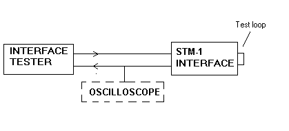
A theoretical draft of the instrumental measurements:

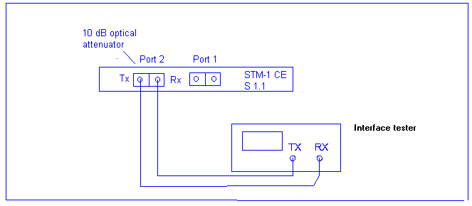
Draft of the real measuring alignment:

Short summary of the operation of the interface as receiver:
Line Rx (receiver) conditions the PCM signal provided by the interface tester, recovers the clock signal from it, decodes line coding and regenerates it by sampling.
Deframer cut off header from the received E1 frames and forwards the contain of the remaining time slots to the ATM Termination Functions modul. Here E1 signal steam will be transformed to a stream of ATM AAL1 frames.
The swithing field of MSS (SC) switches the AAL1 frames arriving from the management and labelled with ATM VPI and VCI towards the destination interface. The E1 - AAL1 conversion can be made for the full frame (ustructured mode) or by time slots (64 kbit/s structured mode). For the VoIP only the second method cvan be used.
The Rx Overhead modul of interface checks frame synchonization, monitors bit errors (CRC-4) within the frame, indicates the received alarms (AIS, RAI) towards mangement and handles service channel.
Short summary of the operation of the interface as transmitter:
The AAL1 frames arriving from the SC will be converted into E1 signal stream by ATM Termination Functions modul, then Framer puts them into the time slots of the E1 frame to be transmitt based on the VPI and VCI. The contain of the 0. time slot will be compiled by the Tx Overhead modul.
The output signal of the interface will be made by line coding by the Line Tx modul.
- 3.1 Testing of the electrical characteristics
- 3.1.1 Signal shape testing
The object of the test is the line transmitter of the interface (Line Tx) which determines the quality of the PCM signal transmitted by the interface. The measuring signal origins from the interface tester, received by the line receiver of the interface (Line Rx). This signal is connected - looped back - to the input of the line transmitter.
Loopback can be activated in the AMS: PDH2 Sublayer/Loopback -> Line. The mask function can be actived in the oscilloscope with the help of the SETUP/SEQUENCE MENU button. For the examination of the signal shape we must use the STEP 4 masking! We should pay attention to the joint closing of the interface (measuring head of 120 Ohm which is the same as the input impedance of the interface tester)! During the measuring the multiplication of the signal with a constant is allowed!
- 3.1.2 Output jitter
Measure the output jitter of the E1 interface!
Now, the object of the test is the line transmitter of the interface (Line Tx), which determines the phase jitter of the PCM signal transmitted by the interface. The measuring signal in this test is the (jitterless) PCM signal provided by the protocol tester and received by the line receiver of the interface (Line Rx). This signal will be connected - loopbacked - to the input of the line transmitter for the measurement.Loopback can be activated using the AMS: PDH2 Sublayer/Loopback -> Line.
Measuring signal must be given from the transmission unit of ME520B. ME520B provides only unframed measuring signal and the interface under test considers this as a wrong signal (Operational State=Down) because its operation mode is framed. However, we do not need to pay attention to the change of the framing type of the interface, because Line Tx and Line Rx remain operational.
Jitter must be analyzed with the receiving unit of ME520B. Set the measuring domain of the jitter according to the measured value!How will reduce the value of the jitter, if we filter the contents with low frequencies?
- 3.1.3 Input jitter endurance
Check that wether the input jitter endurance of the E1 interface corresponds to the minimum specification at 10 kHz or not.
Now, the object of the test is the line receiver of the interface (Line Rx). The measuring PCM signal containing jitter provided by the tester. In order to recognise the errors the signal received by the line receiver will be connected - loopbacked - to the input of the line transmitter for the measurement.Loopback can be activated using the AMS: PDH2 Sublayer/Loopback -> Line.
Measuring signal must be given from the transmission unit of ME520B. The modulating signal will be generated with the EMS 10 equipment.
ME520B provides only unframed measuring signal and the interface under test considers this as a wrong signal (Operational State=Down) because its operation mode is framed. However, we do not need to pay attention to the change of the framing type of the interface, because Line Tx and Line Rx remain operational.
Errors must be counted with the receiving unit of ME520B.
How much is the input jitter endurance of the interface is better than th minimum specification? - 3.1.4 Bit rate test
Check, if the bit rate of the PCM signal given by the interface is within the tolerance or not?
Bit rate (and together with it the clock signal generator of the interface) must be within the same value domain, so that the bit-synch between the interfaces could be realized.Determination of the bit rate of a signal given by the interface is in menu point of HP37732A Result: BER MEASUREMENTS Display:SIGNAL.
During this test we must take care of, that the transmission unit of the tested interface could get the timing signal from the own clock of the MSS (PDH2 Sublayer/Tx Clock Source -> Netsync)! Loopback must be switched off in the AMS: PDH2 Sublayer/Loopback -> Off.
- 3.1.1 Signal shape testing
- 3.2 Functional tests
During these tests we do not measure electric signal, but we examine, if the interface operates appropriately, or not.
- 3.2.1 Testing frame types and line coding
Examine the behavior of the interface if the frame type or line coding of the received signal is incompatible (Rx overhead processor and Line Rx test).
Let we set incompatible fram types and line coding methods (E.g: given frame: PCM31, expected frame: PCM31_CRC or line coding of the transmitted signal: HDB3, expected line coding: AMI) at the HP37732A interface tester, and at the examined PCM interface, and then examine the maintenance signals of the interface, whether they could indicate the incompatibility. The maintenance signals of the tested inteface can be seen in the AMS->Event&Alarm->Current_Alarm_List menu. Clicking on the relating line the detailed alarm signal can be read.
We should report an issue like this.
- 3.2.2 Testing the header (overhead) of the frame (FAS, NFAS)
Examine if the content of the 0. time slot in the PCM signal transmitted by the interface corresponds to the standard, or not. (Tx overhead processor test)
We could make this examination at the menu of the Results: Timeslot Monitor of HP37732A.
- 3.2.3 Test of frame synch
Check the appropriate operation of the frame synchronous algorithm. (Tx, Rx overhead processor test)
We can make the examination using the HP37732A Settings: 2Mbit/s FMSIM measuring mode. Here, setting the test: FAS WORD mode we can put errors into the given frame synch code words. The test should be started from the errorless situation, then the amount of the errors should be increased until the loss of the synch. After that we should decrease the the amount of the errors until the recovery of the synch. The maintenance signals of the tested inteface can be seen in the AMS->Event&Alarm->Current_Alarm_List menu. Clicking on the relating line the detailed alarm signal can be read.
- 3.2.4. Loop back one (or some) time gaps of the tested E1 interface with the help of the AXD SC.
WIth this examination we can check the Framer and Deframer functions of the interface.Beside this It provides an insight into the operation and user level programming of the switching field (SC) and the TDM/IP converter called Media Gateway of the MSS. With the help of the AMS find out that to which MSS application is the the tested interface assigned and where the several time slots of the tested inteface are connected? Fill out the empty column of the following table:
Attribute Possible set of the values Recent value Is a CE application? yes / no Is a Voice application? yes / no Is a Media Gateway Device? yes / no Media Gateway Name b211, b212, b213 Connected time slots E.g.: 6-7, 1-2... The above mentioned information can be read in the following menus:
- Switch_Fabric/Circuit Emulation -> Open CESes ->Does the tested interface appear between the interfaces assigned to the circuit emulation interfaces?
- Voice/Media Gateway -> Open Devices -> Is the the tested interface assigned to a Media Gateway and through this to a "Voice" application?
- Voice/Media Gateway -> Semipermanent connections -> List about the connected time slots.
We can perform out the test with previously connected time slots, but in the Create Semipermanent connections menu we can create a connection between the two time slots of the tested interface, too. We can check the operation of the test alignment with the bit errors put into the measuring signal (Continuity test)!
- 3.2.1 Testing frame types and line coding
The STM-1 interface of the MSS has a significantly higher capacity than E1 interface,
because it is able to multiplex/demultiplex and transmit/receive 63 pieces of E1 signals
to/from external exchanges.
Accordingly, the STM-1 interface has a more complex (a more layered) structure than E1.
In the orientation of notations of the several components of the STM-1 used in the Tutorial
and in the AXD AMS will help us the following table:
| SDH layers (Tutorial) | sublayer name (AMS) | interface type (AMS) | Frames, Containers | Overheads |
|---|---|---|---|---|
| circuit layer | E1 interface | PDH | here it is E1 | TS0=FAS, NFAS |
| lower order path layer | VC-12 interface | SDH LOW PATH (LP) | LOVC here it is VC-12 | POH |
| high order path layer | SDH path interface | SDH PATH (HP) | HOVC here it is VC-4 | POH |
| transmission media layer | SDH interface | SDH | here it is STM-1 | SOH=RSOH+MSOH+AU4P |
- 4.1. With the help of the AMS identify the operation and state parameters of the
appointed STM-1 interface of the MSS and fill the table:
STM-1 interface (SDH interface sublayer):
Attribute Possible set of the values Recent value Is the interface (link) available? yes? no? Does the interface (link) operable? If not, what is the cause? yes? no? Transmission frame format SDH? SONET? Line coding NRZ?, Transmission clock source internal?, Rx? Implemented maintenance signals LOS?, AIS?, RDI? ...? Loopback off?, line?, local? - 4.2. With the help of the AMS identify the operation and state parameters of the interface of (E1) subport to be multiplexed into the frame of the appointed STM-1 interface of the MSS and fill the table:
E1 interface sublayer
Attribute Set of the possible values Recent value Is the interface (link) available? yes? no? Does the interface (link) operable? If not, what is the cause? yes? no? Transmission frame format PCM 30/31?, CRC? Line coding AMI?, HDB3? Transmission clock source internal?, Rx PCM? Implemented maintenance signals LOS?, AIS?, RAI? Loopback off?, line?, local? - 4.3 To find the above mentioned information follow these steps:
- AMS -> Equipment/Configuration -> Equipment/Configuration (command menu) -> Open Equipment Modules
- Equipment Management/Equipment Modules (EM directory) -> Selection of the EM belonging to the interface
- Equipment Management/Equipment Module (EM panel) -> Open Links
- Link/Links (Link directory) -> Selection of the link belonging to the tested interface
- Link/Link Data - STM1 -> Administrative attributes of the link belonging to the tested interface -> Show detailed link data
- Link Data/Link Details -> Reading the attributes of the tested interface (SDH interface sublayer)
- Link/Link Data - STM1 -> Open sublinks
- Link/Sublinks (Sublink directory) -> Selection of the sublink (port) to be multiplexed
- Link/Sublink Data -> Administrative attributes of the sublink (port) to be multiplexed -> Show detailed sublink data
- Link Data/Sublink Details -> Reading the attributes of the sublink (port) to be multiplexed (SDH interface sublayer)
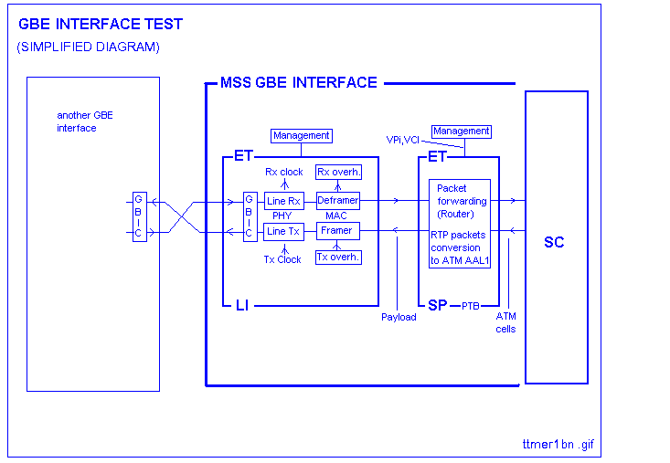
The instrumental testing procedures (signal shape, phase jitter, and fuctional tests) of the GBE interface are similar to the testing procedures of the E1 interface. A principled draft of the measurement:
The fundamental difference is that testing of STM-1 requires two orders of magnitude higher speed measuring equipments than in the case of E1. Dashed line on the above figure indicates the lack of the oscilloscope having high rate optical inputs.
Draft of the functional measuring alignment:

- 5.1 Testing of the electrical characteristics
Because of the lack of the testing tools we can not examine electrical caracteristics (signal shape, phase jitter, etc.) at this interface.
- 5.2 Functional tests
For the funcional testing of the STM-1 interface HP37724A interface tester will be used. The test cases selected for this task are mostly STM-1-specific.
- 5.2.1 Preliminary settings
In order to perform the test cases we have to set STM-1 interface of the HP37724A equipment according to the configuration of the tested interface. In this will help the following table:
Parameter Transmit menu
Main SettingsReceive menu
Main SettingsTransmit/Receive Signal STM-1 OPT STM-1 OPT Payload TU-12 TU-12 TU mode async async Selected TU 1.1.1 1.1.1 TU Payload int CRC4 int CRC4 Timeslot all ts all ts Pattern 2^15-1 2^15-1 After setting the above parameters measuring equipment will transmitt/receive STM-1 frames on its optical interface. It multiplex a TU-12 component into the VC-4 container (into the first position (1.1.1) from the possible 63). Into the TU-12 components itmaps asynchronously 4-4 E1 frames. The source of the E1 frames is the HP37724A tester, too. (Internal payload generator). E1 frames contain CRC4 multiframe in their 0. time slots, while in the 1-31 time slots segments of a 15-bit PRBS signal will be transmitted. The receiver of the equipment waits for the errorless transmitted signal.
The received signal will be errorless if the tested interface loops back the test signals. There is two loopback possibility on the tested interface, please use the following settings:
- SDH interface sublayer - Loopback off
- E1 interface sublayer - Loopback line
As we do not use the SDH interface sublayer loopback it is possible to test line and multiplex part jointly.
Finally, please, check the interconnection of the measuring equipment and the tested interface according to the next figure::
10 dB optical attenuators are important parts of the interconnections, becasuse they prevent the overdriving and the consequent untimely failure of optical receivers.
After completion of the above settings we can start with functional tests.
- 5.2.2 Error and Alarm test
During the test interface tester transmits STM-1 frames containing errors and alarms and we will observe the behavior of the interface under test when receiving these frames.
Insertion of errors and alarms can be done in the Transmit/Test function/Errors & Alarms menu of the interface tester. The maintenance signals of the interface under test can be seen in the AMS->Event&Alarm->Current_Alarm_List menu. (After the click we have to wait for a while.)Clicking on the relating line the detailed alarm signal can be read.
Suggested test, as an example: transmit frames containing MS-AIS.
Suggested optional task: STM-1 frame synch test.
Reporting: maintenance signals (alarms).
- 5.2.3 Studying of the overheads (STM-1 SOH, VC-4 POH, VC-12 POH)
The content of the overhead of frames of the tested interface can be studied using the tutorial (links can be find above). Interface tester provides the following possibilities for the testing:
- Transmit/Section overhead menu: We can manipulate the header bits of the STM-1 frames given by the tester
- Transmit/Path overhead menu: We can manipulate the header bits of the VC-4 frames given by the tester
- Receiver/SOH monitor menu: We can monitor the header bits of the STM-1 frames given by the tested interface
- Receiver/POH monitor menu: We can monitor the header bits of the VC-4 frames given by the tested interface
- Receiver/Test Function/Overhead Capture menu: We can capture the header bits of the STM-1 frames given by the tested interface
After studying answer the following questions:
- Is there any significant difference between the frame synch procedures of E1 and STM-1 frames?
- What line error detection methods are applied in the E1 and STM-1 frames?
Using the above mentioned possibilities collect and write out the all trace identifier and signal label values given by the tested interface!
- 5.2.4 STM-1 optical interface clock recovery test - Stress test
In this task we can test that how long series of bites of 1s or 0s cause loss of bit synch in the clock recovery circuit of the receiver of the tested STM-1 optical interface. In this case tester inserts series of bytes of 1s or 0s with programmable length into the STM-1 frames - simulating short time break downs.
The insertion can be made using Transmit/Test Function/Stress Test menu.
Examine how long series of bytes of 1s or 0s cause disorder in the operation of the tested interface?
- 5.2.5 Pointer processing test (AU-4 PTR, TU-12 PTR)
In SDH frames (STM-1, TU-12) position of the payload (VC-4, VC-12) frame is unbound, it can vary. The start of the payload described to frame by pointers (AU-4 PTR, TU-12 PTR). Pointers receive value at the start of the operation of the interface and this value remains unchanged in the case of normal operation.
In the case of difficulties in timing or clock signal provisioning it may occurs that frame and payload are driven by different timing source: payload "moves" inside the frame. The interface seeks to compensate this phase shift by overriding the value of the pointer.
During the test interface tester transmit STM-1 frames in which there is rate difference between the clock sources of the frame and the payload (offset).
The above mentioned signal can be generated in the Transmit/Test function/Adjust pointer menu.
Examine how much offset causes disorder in the operation of the tested interface?
As a farewell to the above interfaces make an interconnection between the measuring connections used in Task 3 and Task 5 with the help of the AXD SC switch using the Task 3.2.4 as an example! Do not forget to switch off loopback at the STM-1 interface!
Reporting: connected ports, time slots, the result of the continuity test in both directions.
The MSS GBE interface has a significantly greater capacity than STM-1 interface becasue it able to transmit/receive ca. 9000 voice channels to/from external exchanges. Nonetheless, GBE interface is more simple than STM-1, it is only a little bit more complicated than E1.
- 6.1. Determine the operation mode and statement parameters of the designated GBE interface of MSS with the help of the AMS. Fill out the empty column of the following table:
Attribute Set of the possible values Recent value Is the interface (link) available? yes? no? Does the interface (link) operable? If not, what is the cause? yes? no? Connected optical fiber? monomode/multimode? Optional interface procedures? - 6.2 To find the above mentioned information follow these steps:
- AMS -> Equipment/Configuration -> Equipment/Configuration (command menu) -> Open Equipment Modules
- Equipment Management/Equipment Modules (EM directory) -> Selection of the EM belonging to the interface
- Equipment Management/Equipment Module (EM panel) -> Open Links
- Link/Links (Link directory) -> Selection of the link belonging to the tested interface
- Link/Link Data -> Administrative attributes of the link belonging to the tested interface
- Link Data/Link Details -> Reading the attributes of the tested interface (Attributes of the GBE interface)
The instrumental testing procedures (signal shape, phase jitter, and fuctional tests) of the GBE interface are similar to the testing procedures of the E1 and STM-1 interface. The fundamental difference is that in this case we do not have any equipment, neither an interface tester, nor a traffic generator for the testing of the GBE interface.
This insufficiency can be bridged by interconnecting two GBE interfaces and the tests can be executed on the link established in this way.
Draft of the real measuring alignment:
- 7.1 Testing of the electrical characteristics
Because of the lack of the testing tools we can not examine electrical caracteristics (signal shape, phase jitter, etc.) at this interface.
On the other hand, type and particle number of the GBIC can be read in the AMS. Using the e.g. Google web search we can find the data sheet of the optical transmitter/receiver of the GBE interface. When studying this datasheet we can conceptualize which parameters may be tested here. To confirm that task was done fill the empty column of the following table:
Parameter Value Data Rate Tx Eye Opening PECL Signals Amplitude PECL Signals Impedance Power Voltage Range Current Consumption - 7.2 Functional tests
- 7.2.1 Alarm test
The maintenance signals implemented on the interface under test can be found in the tutorial.
We may generate alarm e.g. by the shut down of the remote interface. The pulling out of the optical fiber from the GBIC is strictly forbidden! Furthermore, this is an active link of the telecommunication test network of the department, which means that the link error may influence the work of the other students! So please take care about this task and consult with the teacher!
The maintenance signals of the interface under test can be seen in the AMS->Event&Alarm->Current_Alarm_List menu. (After the click we have to wait for a while.)
- 7.2.2 Error analysis
Frame errors detected by the interface as well as statistics relating to the transmitted and received frames can be studied in the
Link Data / Link statistics
menu of the AMS.
- 7.2.1 Alarm test
The maintenance signals implemented on the interface under test can be found in the tutorial.